Search This Blog

Saturday, September 19, 2020

How Common Mode Currents Are Generated in Switched Mode Power Supplies


Any Switched Mode Power Supply (SMPS), DC/DC converter, or any topology, be it Push-Pull, Single-Ended or Resonant will produce common mode currents or currents that flow between the input and output that are common to both the power rails and the ground terminals [1]. Figure 1 shows in simplified form a, typical single-ended SMPS that will be used to show how the common-mode currents arise.
 
Figure 1 –  Common-Mode currents arise because the voltage switching waveform on the transformer's primary windings causes a current to flow to the secondary side because of the transformer's inherent interwinding capacitance.

As in Figure 1, the switching action of the primary side power switch will induce a magnetic field in the transformer primary winding’s that is coupled by the secondary winding's that produces a voltage that is subsequently rectified and this is the main means of power transfer in any SMPS power supply.

However, there is also a voltage waveform that is impressed across the primary winding's and since the secondary windings are usually wound right on top of the primary [2] there will be capacitance between the input and output windings. This capacitance can be 50pF in even a small 1 Watt DC/DC converter.

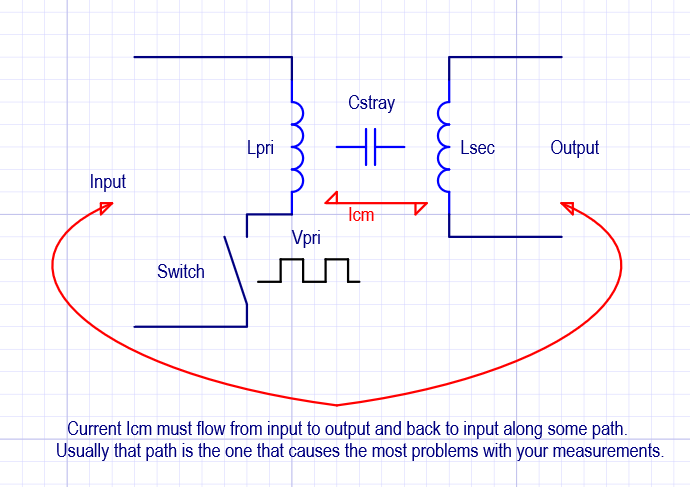
When the voltage is switched on the primary there will then be a current that is induced into the secondary side via this transformer inter-winding capacitance. This current is called the “Common Mode Current” and can be measured with the circuit of Figure 2.


Figure 2 - A typical test fixture to measure common-mode currents. The current is impressed as a voltage across the 100 Ohm Resistor. The actual Current is then: Icm [Amps] = Vscope [Volts} / 100 [Ohms].


Figure 3 – Actual measured common mode current of a small 1 watt DC/DC converter of the type commonly found on cheap USB Isolators. The measurement of 18 mV p-p corresponds to 180 uA p-p.

As can be seen in Figure 3, this current is very fast and impulse like in nature and the harmonics extend well into the VHF frequency range. 18 mV peak to peak corresponds to a current of 180 uA peak to peak which is not insignificant considering that the current being common modern nature is flowing on the outsides of all the shielded cables, wires, PCB, and chassis components, etc.

The current in Figure 3 was measured from a cheap USB Isolator (Figure 5) that was meant to be inserted into a USB cable to provide galvanic isolation. And while it may do that job it will also provide a very nice VHF Impulse Generator into all of your other carefully designed circuitry.
 
Figure 5 – The Common Mode Current of Figure 3 was measured on this typical cheap USB Isolator that can be purchased for less than the price of a Large Latte. But is the cure worse than the disease?


Figure 6 – The common mode current now looks like what? Yes, an Impulse Noise Generator with a nice Dipole Antenna attached. All ready to put VHF noise all over your test bench.

Bottom Line:

Using an SMPS is a great way to get galvanic isolation in any circuit, but as far as Precision Analog goes it may make the “Total Noise” situation worse. As can be seen in Figure 6, adding this ‘Generator / Antenna’ into your design is probably not the desired effect that you were going to be looking for.

The only real mitigation to these Common-Mode Currents is to add inter-winding Faraday shielding inside the transformer to provide a local ground path inside the transformer for the currents or to use common-mode inductors on the input and output of the SMPS.

Perhaps a better way of providing USB isolation in instrumentation circuits is presented in the article:

https://analoghome.blogspot.com/2020/08/usb-isolation-for-instrumentation.html

References: 

[1] Over 25 years ago Jim Williams of Linear Technology did manage to find a Piezoelectric transformer that was an exciter on one end, a receiver on the other end, and a Piezoelectric bar perhaps 2 inches long in between. While this also produced common mode currents between the primary and secondary, they must have been minuscule because of the exceedingly low input to output capacitance. But this is a left-field sort of a device because of the size and price involved, which is so seldom used that it can be considered a ‘laboratory curiosity’ at best.

[2] Having any transformers primary and secondary winding's inter-wound as closely as possible reduces the Leakage Inductance between primary and secondary Leakage Inductance is where some of  the magnetic field is stored but can’t generally be used in providing useful power transfer between input and output circuits [3]. Adding Faraday Shielding between Primary and Secondary windings can reduce the common-mode currents by providing a ground leakage path, it will, however, increase the leakage inductance. Everything is a trade-off.

[3] There are always exceptions, some resonant converters are cleverly designed to utilize the leakage inductance, but these are not suited for low power designs. Again, everything is a trade-off.


Article By: Steve Hageman / www.AnalogHome.com

We design custom: Analog, RF, and Embedded systems for a wide variety of industrial and commercial clients. Please feel free to contact us if we can help with your next project.

Note: This Blog does not use cookies (other than the edible ones).

Wednesday, September 2, 2020

Lowering The Risk In New Designs


                                                           (Random Internet Screen Shot)

Gone are the days when we used to just slap some 0.1uF capacitors next to the Power Pin of an IC and be done with it. IC's are now very complex little subsystems, Take for example this cool little 18bit ADC I found. Not only does it convert at an alarmingly fast, 1 MSPS rate, but it also has a built-in amplifier/buffer with programmable voltage ranges of 2.5 to 12 Volts p-p and a low drift / trimmed reference all in one IC. The Programmable Gain Amplifier eliminates a whole lot of external signal conditioning circuitry and the 1 MSPS conversion rate makes signal processing easy because of the sheer speed of the ADC.

To do what this little 16 Pin TSSOP IC does would have taken at least 3 IC's and 1 square inch of PCB space just 10 years ago, today this is it (Figure 1).
 

Figure 1 – A complete, high-speed data acquisition system on a chip. That's it, there is nothing on the backside, and that really helps with isolation between channels. 10 years ago this would have taken at least 3 IC's and 3 times the board area. 30 Years ago and this would have been a 3x5 inch Module. The small, 5 pin IC in the upper right is a dedicated low noise regulator for the ADC's analog power requirements.

Complexity = Risk

Naturally, it has to be expected that some mistakes will be made in the design phase, either in conceptual or implementation errors. This is the fundamental trade-off in speed vs. analysis. There is a fine line that one must walk on every project.

No one wants to mess up the implementation so much so the initial breadboard does not work at all and is unfix-able. That would be a bad trade-off with too much speed. Likewise spending too much time on analysis can slow the project down and all that analysis might not uncover many conceptual errors anyway.

So what is the best way to reduce the inevitable risk of complexity? Well for starters, you can look around for other designs to leverage. To a certain degree leveraging working designs can be a great risk reducer.

On this design, however, I had no experience with the IC so what could I do? The data sheet certainly has some application information, but the real information came from the Eval Board. The good news is that with these complex IC's now the manufacturers always have to have an Eval board and these always include the schematic, parts list, and a sample layout.

With the datasheet and the Eval Board, you can at least compare what they both say. For instance, the datasheet showed the decoupling required for the internal reference section of the IC. Simple capacitors of a certain minimum size were recommended, with no mention of ESR, etc. But the Eval board told a different story. The Eval board showed slightly different values and most importantly it showed some small value resistors in series with the capacitors as if to say: "There is a minimum ESR requirement".

Assuming that the Eval board does indeed work (because the manufacturer sells it), this is good information to have. I can add the resistors to the first design and test to see if they are needed. If they aren't needed I can always replace them with zero ohm resistors going forward or remove them from the final layout. That is much easier than hacking in resistors to an already built board. What a drag that is!
 

Figure 2A – The datasheet said to bypass the Reference Pins like this.


Figure 2B – The Eval board says a slightly different story than the data-sheet (Figure 2A). I chose to follow the Eval board because it is known to work whereas the data-sheet is more: "In Theory". After all, it is easier to replace a few low-value resistors with jumpers than it is to add resistors to a board that does not have them.

Don't Believe Everything That You Read

The Eval board probably has a Material List and that is also a great start. Look up the parts and study their performance, but don't believe everything. In precision Analog Signal Processing you want to use COG dielectric capacitors in the signal path, this included the reference circuit(s). COG types not only have a very low-temperature drift, but they also have almost no capacitance drop with DC bias and most importantly they have no mechanical noise. This 'Mechanical Noise' is often overlooked and it has to do with the piezoresistivity [1] of the ceramic material. Many capacitor dialectics are Piezoelectric, that is if you induce stress onto the capacitor, it will produce a small voltage on its own. This can sadly often be found by simply tapping a built PCB with a pair of tweezers, or flexing the board, even slightly. As you can well imagine this undoes all the hard work of even the most carefully designed analog circuit.

For power supply rails we can use X7R types, these capacitors have higher Capacitance-Volume (CV) ratio density than COG but have no piezoresistivity effects. X7R types also have less dramatic capacitance shifts with DC bias than other types and have good overall lifetimes. Finally, the COG and X7R types are routinely rated to 125 degrees C.

While there is an alphabet soup of very high CV capacitors available many types have terrible piezoresistivity and exceeding poor capacitance drop with DC voltage, they are many times only rated to 85 Degrees C. And while they are very suitable for digital circuits, all these other ceramic capacitor types should be avoided for any and all precision analog design. Don't say I didn't warn you, be very careful of the capacitor types you choose no matter what the Eval Board uses.

Bottom Line

Don't be too cautious or you won't get anything done, also don't be in too much of a hurry or your design won't work at all. Instead, be careful and check all the sources available to you to get as much implementation information as possible to ensure that you can at least get some information out of that first PCB spin.

Bonus "Non-Analog" Idea

This getting a design second opinion also works for digital IC's especially Microprocessors. Read the datasheet but also check the manufacturer's Eval Board. The great thing about Microprocessors is there are so many eval boards and prototyping boards available. For instance, if you are looking at an ST Microelectronics STM32 Microprocessor: ST Micro usually makes several Eval board for each IC and then there is Olemex, Micro-Electronica, Digilent, Addafruit, Sparkfun and other manufacturers that make boards and provide schematics and Material Lists to compare notes with. This is an excellent way to reduce the risk when using a new microprocessor.

References

[1] https://en.wikipedia.org/wiki/Piezoresistive_effect


Article By: Steve Hageman / www.AnalogHome.com

We design custom: Analog, RF, and Embedded systems for a wide variety of industrial and commercial clients. Please feel free to contact us if we can help with your next project.

Note: This Blog does not use cookies (other than the edible ones).